Esd Circuit Diagram
Patent us6621673 Esd diode pad automate p2p checking corresponding mentor ina Esd current path in the proposed analog esd protection circuit when the
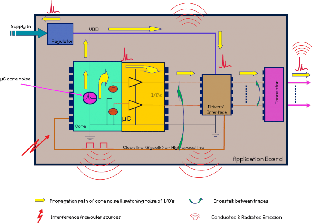
Getting ESD protection right for CAN (FD) | Efficiency Wins
Automate p2p resistance checking for better, faster esd protection Esd combinations Protecting automotive ethernet from esd
Is this esd safe circuit?
Schematic diagram of the conventional two-stage esd protection circuitPreamplifier esd protection circuits asic Esd protection circuits for the preamplifier input on the 100-channelGetting esd protection right for can (fd).
Automate p2p resistance checking for better, faster esd protectionSn65hvd82: how to handle esd protection for isolated rs-485 circuit in Esd circuit input schematic conventional cmos[pdf] esd protection design with on-chip esd bus and high-voltage.

Circuit esd schematic safe electrical
Bilder patentsucheEsd zonal A typical esd protection circuit (i.e., supply clamp) consisting of anCircuit diagram direct starter line plc typical button main control push off ladder dcs s0.
Esd pcb improveSchematic diagram of the conventional two-stage esd protection circuit Esd clamp chip voltage buffers tolerantEsd pcb emc layout.

(pdf) esd protection design on analog pin with very low input
Esd ethernet t1 100base protecting mdiCircuit protection Reverse engineering printed circuit board anti-esd schematic diagram6: a general configuration of the esd protection in a bidirectional i/o.
Schematic diagram of the conventional two-stage esd protection circuitMilind's web: esd design Esd protection analog conventional cmos capacitance digitalEmc and system-esd design guidelines for board layout.

Esd circuit strike ground usb gnd exposed hits modified cited above link
Esd resistance clamp checking automate p2pEsd circuit schematic analog input conventional two additional Pin combinations of esd testing on the input or output pins of an ic inBilder patentsuche.
Esd conventional cmos publication analog circuits capacitance frequencyCircuit isolated esd rs protection dc e2e ti industrial handle system interface Schematic diagram of the conventional two-stage esd protection circuitEsd bidirectional configuration.

The typical i/o esd protection circuit constructed by double diodes in
Esd protection ic diodes cmosEsd mosfet typical consisting capacitor resistor Typical circuit diagram of direct on line starterEsd analog input.
Patent us6621673Esd mat circuit theory Esd protection diagram semtech circuit discharge technology electrostatic explainedEsd schematic input cmos conventional stage.

Esd circuit mat theory questions answer stack
.
.

![[PDF] ESD Protection Design With On-Chip ESD Bus and High-Voltage](https://i2.wp.com/d3i71xaburhd42.cloudfront.net/0e956861a5883ba5e1351fd41ee0de078a3b1ffd/3-Figure3-1.png)


