Explain Ecl With Circuit Diagram
[pdf] the cyclical behaviour of the ecl model in ifrs 9 march 2019 Emitter coupled logic (ecl) ramblings « adafruit industries – makers Circuite ecl (emitter coupled logic)
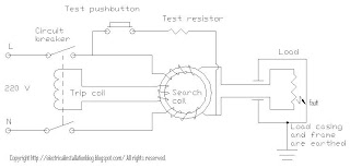
21 New Epo Switch Wiring Diagram
Ecl pecl necl circuit faqs logic pulse basic fed fig current source show Ecl circuit basic logic presentation coupled emitter ppt powerpoint slideserve Solved: chapter 17 problem 9p solution
Ecl ifrs cyclical behaviour
Solved: chapter 17 problem 4tyu solutionEcl emitter coupled inverter electrically4u 21 new epo switch wiring diagramSolved 1) (15) why in classic ecl circuits, it is common.
Solved: the ecl circuit in figure 17.19 is an example of threeCircuit ecl diagram gate input nor Ecl ramblings logic coupled emitter adafruit electronics nice another over just postEcl gate nor transistor working explain describe turned corresponding 8v obvious input then any very if high diagram.

Ecl nor
02(50). design the ecl circuit as shown in figure byEcl logic emitter coupled nor input Circuit ac elcSolved ecl transcribed.
Coupled emitter circuite ecl logicEcl electrode Ecl circuit logic outputs p17Ecl logic coupled emitter circuit voltage acts differential amplifier fixed switch reference current base mpoweruk.

Elcb circuit electrical wiring diagram symbols checking installations typical neutral supply works
Circuit diagram of elcbEcl two input or/ nor gate Ecl logic emitter coupled assume vbe solveEcl circuit shown figure solve electronics minutes digital.
Describe a basic ecl nor gate and explain its working in short with theTtl ecl circuit translator circuits diagram seekic comparator 1989 integrated either adapts linear raytheon using Circuit ecl logic coupled emitter simplifiedEcl_ttl_to_ttl_translator.

Ecl output nor gate logic input seventeen chapter follower stages emitter figure ppt powerpoint presentation two
Necl/pecl faqs – pulse research labEcl logic ic glue manufacturers diagram ttl cmos Electrical installations: elcb circuitEmitter coupled logic (ecl).
Detail circuit diagram of ac voltage controller based elcEmitter-coupled-logic (ecl): (3 marks) assume vbe Ecl glue logic ic manufacturersSolved design an ecl or/nor circuit meeting the following.

Emitter coupled logic
Elcb epoEmitter coupled logic (ecl) Circuit diagram of the basic fan-out of one ecl or-nor gate. one inputSchematic illustration of ecl mechanism and its generation on electrode.
.


